The global demand for advanced microprocessors and memory modules has thrust rare elements into the spotlight. Modern electronics rely on a handful of scarcely available materials whose extraction, processing and integration present both technical hurdles and strategic imperatives. Semiconductor fabs now wrestle with securing stable supplies of metals that are critical not only to chip performance but also to geopolitical stability. This article explores the multifaceted landscape of rare materials in semiconductor manufacturing, examining supply dynamics, environmental implications, innovation pathways and the emerging challenges that shape the industry’s future.
Global Supply Dynamics and Strategic Reserves
At the heart of the semiconductor ecosystem lies a complex web of mining operations, refining plants and distribution networks. Countries like China, Australia and the United States host major deposits of rare elements such as neodymium, terbium, dysprosium and gallium. Despite this, the production chain often funnels through a handful of smelters and purification facilities, creating a concentration risk that can trigger price spikes or export restrictions.
Governments have recognized the need to bolster their supply chains by establishing strategic stockpiles and incentivizing domestic processing capacity. The European Union’s Critical Raw Materials Act aims to ensure that at least 10 percent of Europe’s consumption comes from EU sources by 2030, while the US CHIPS and Science Act dedicates billions to expand local mining and recycling efforts.
- Neodymium and dysprosium: essential for high-strength permanent magnets used in actuators and automation tools.
- Gallium and germanium: key substrates for compound semiconductors in 5G and photonic applications.
- Tantalum and tungsten: critical for producing high-k dielectrics and collision shielding in ion implantation equipment.
To reduce dependency, firms are exploring alternative sources in developing nations, yet obstacles such as inconsistent regulatory frameworks and limited infrastructure often hinder rapid scalability. The result is an ongoing tug-of-war between demand growth—driven by AI, edge computing and electric vehicles—and the capacity to deliver uninterrupted material flows.
Environmental and Ethical Considerations
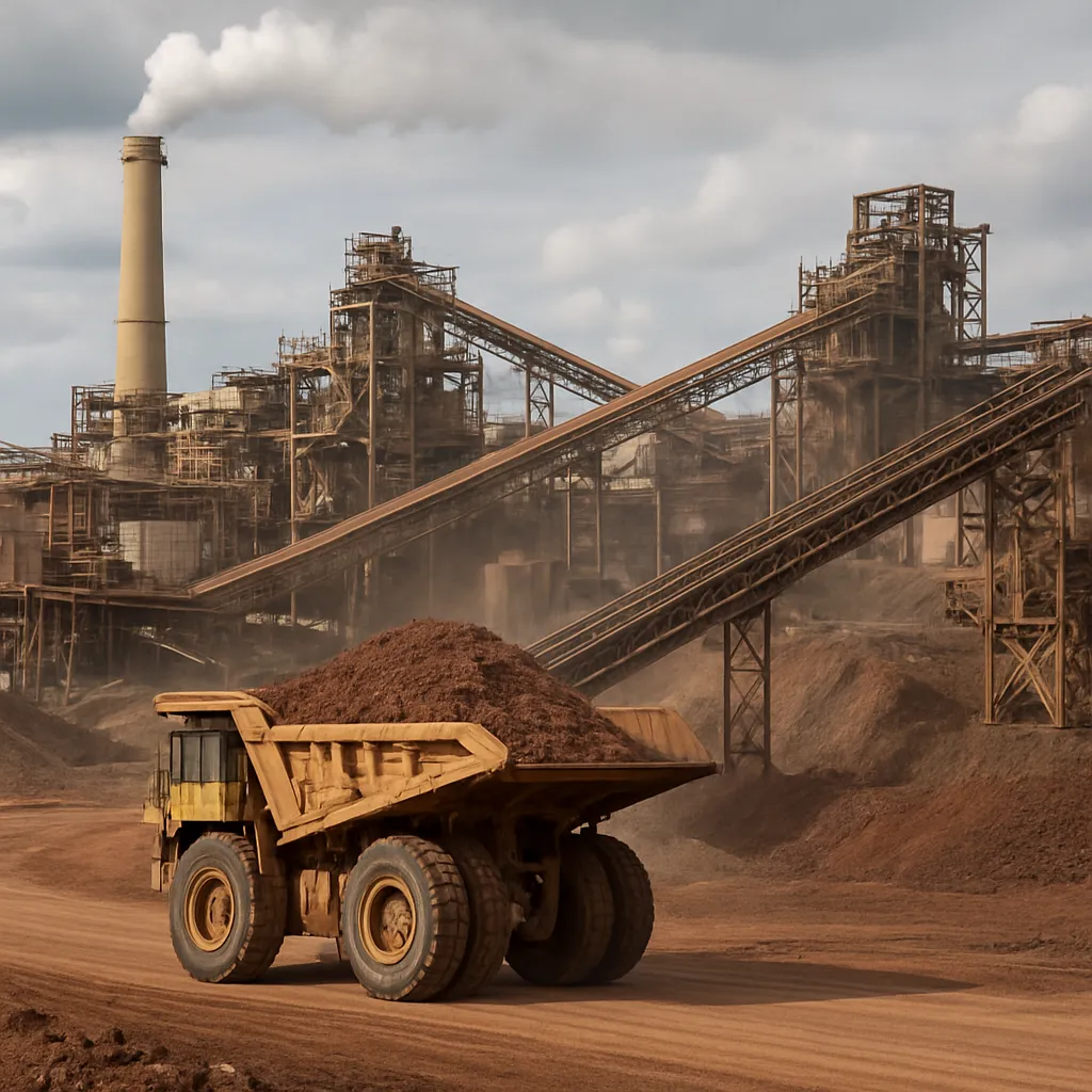
The lifecycle of rare elements exerts substantial environmental pressure. Conventional mining can lead to deforestation, soil erosion and contamination of water resources with heavy metals and processing byproducts. Extracting bauxite for aluminum, for example, often leaves behind vast red mud tailings that, if mismanaged, pose toxic risks to surrounding ecosystems.
Ethical sourcing emerges as a critical priority. Smelters in remote regions may employ energy sources with high carbon footprints or fail to provide adequate labor protections. Leading semiconductor companies are responding with rigorous due diligence and third-party audits to ensure compliance with environmental, social and governance (ESG) criteria.
Key Environmental Challenges
- Water scarcity: Hydrometallurgical operations demand large volumes of freshwater, straining supplies in arid zones.
- Emissions: Roasting and smelting generate sulfur dioxide and other harmful gases unless abated by advanced scrubbers.
- Waste disposal: Persistent tailings require secure containment to prevent leaching of toxic elements.
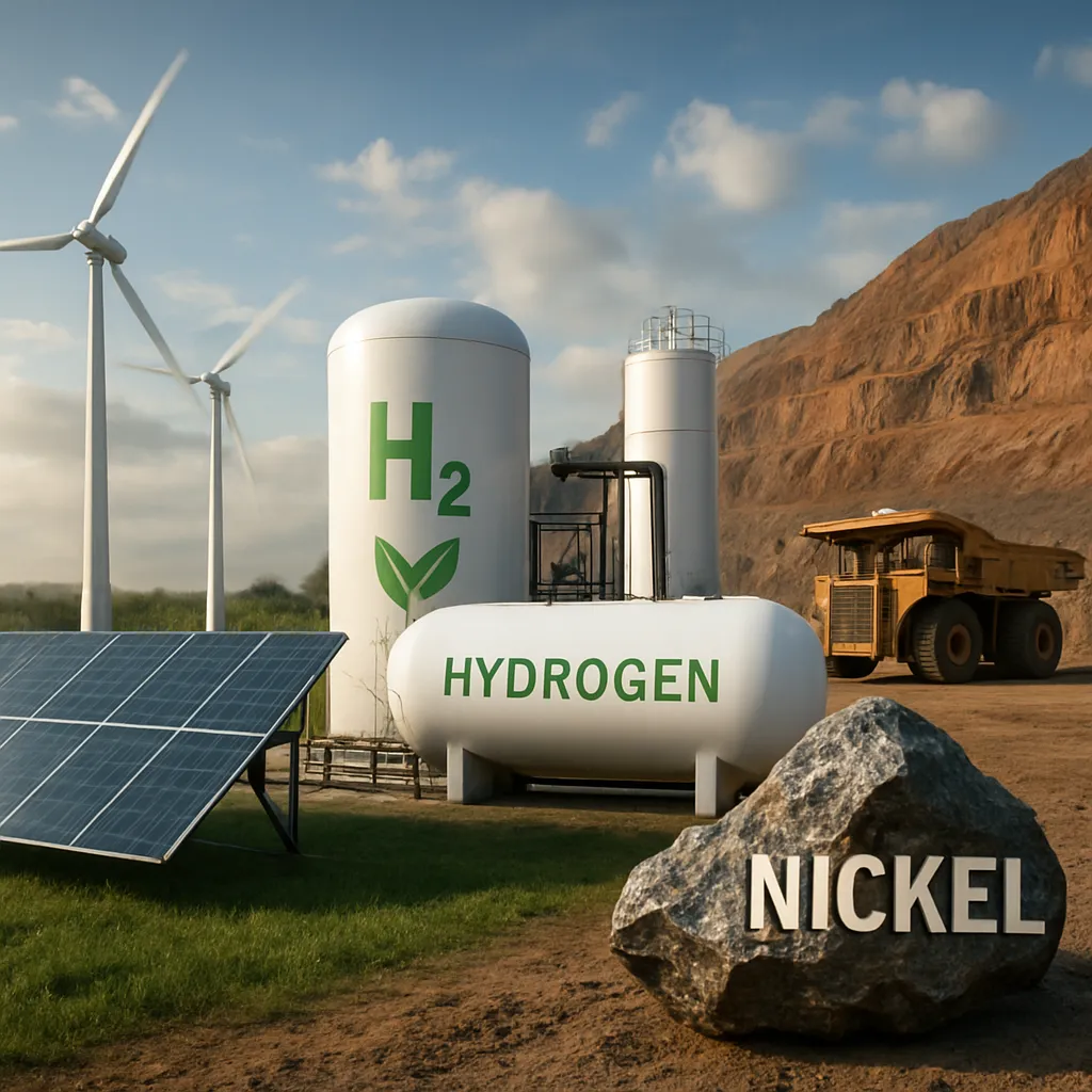
One promising avenue involves bioleaching, where specialized microorganisms extract metals at ambient temperatures, significantly reducing energy consumption. Pilot projects in Canada and Finland have demonstrated success in recovering copper and nickel with minimal environmental disturbance, pointing toward similar applications for metals like cobalt and lithium. Meanwhile, closed-loop water treatment systems are being integrated into new refineries to curtail freshwater usage by reusing up to 90 percent of process water.
Technological Innovations and Substitution Efforts
Innovation remains a cornerstone for mitigating material scarcity. Research teams worldwide are investigating how to replace or minimize the use of certain rare elements without compromising semiconductor performance. Architects of next-generation logic transistors, for instance, are experimenting with alternative high-k dielectrics that reduce reliance on hafnium and zirconium.
In packaging and interconnects, copper pillars are being optimized to supplant silver-based solders, cutting costs and lowering the need for conflict-prone sources. Similarly, advances in additive manufacturing enable precision-engineered alloy powders that improve deposition efficiency, slashing the waste associated with conventional chemical vapor deposition and electroplating processes.
Substitution Strategies
- Alloy engineering: Blending more abundant elements into functional alloys that mimic the properties of rare counterparts.
- Thin-film coating: Leveraging atomic layer deposition to achieve ultra-thin protective layers, minimizing overall material consumption.
- Nanostructuring: Creating nanoscale composites to boost electrical and thermal conductivity, reducing the volume of rare elements needed.
Meanwhile, machine learning algorithms are optimizing crystallization pathways to maximize yield of high-purity semiconductors, trimming off-spec waste. These digital twins of manufacturing lines help pinpoint process deviations early, conserving precious resources and enhancing overall yield rates—key metrics as fabs stretch to 3 nm and beyond.
Geopolitical Tensions and Supply Chain Security
As nations vie for technological sovereignty, geopolitics increasingly shapes rare metal availability. Export quotas, trade sanctions and diplomatic disputes can all disrupt the steady flow of critical inputs. Recent trade frictions between major producers and consumers underscore the vulnerability of lean, just-in-time procurement strategies.
To buffer against such shocks, multinational corporations are diversifying their supplier base and deploying advanced analytics to forecast potential disruptions. Real-time risk management platforms now track political developments, shipment delays and price anomalies, enabling procurement teams to pivot swiftly when alarms sound.
Resilience-Building Measures
- Dual sourcing: Contracting with at least two independent suppliers for each key element.
- Inventory optimization: Maintaining safety stocks strategically positioned near critical fabs.
- Vertical integration: Investing in joint ventures at mining and refining stages to gain direct control over material quality and availability.
Some leading chipmakers have gone further by forging partnerships with sovereign wealth funds and regional governments to co-develop new mining projects. These collaborative models aim not only to lock in access but also to ensure compliance with evolving sustainability standards. In parallel, consortia of fab operators have pooled resources to finance large-scale recycling facilities, chasing a vision of circular economy where end-of-life wafers are deconstructed and their metal constituents reclaimed for new production cycles.
Recycling and Circular Economy Pathways
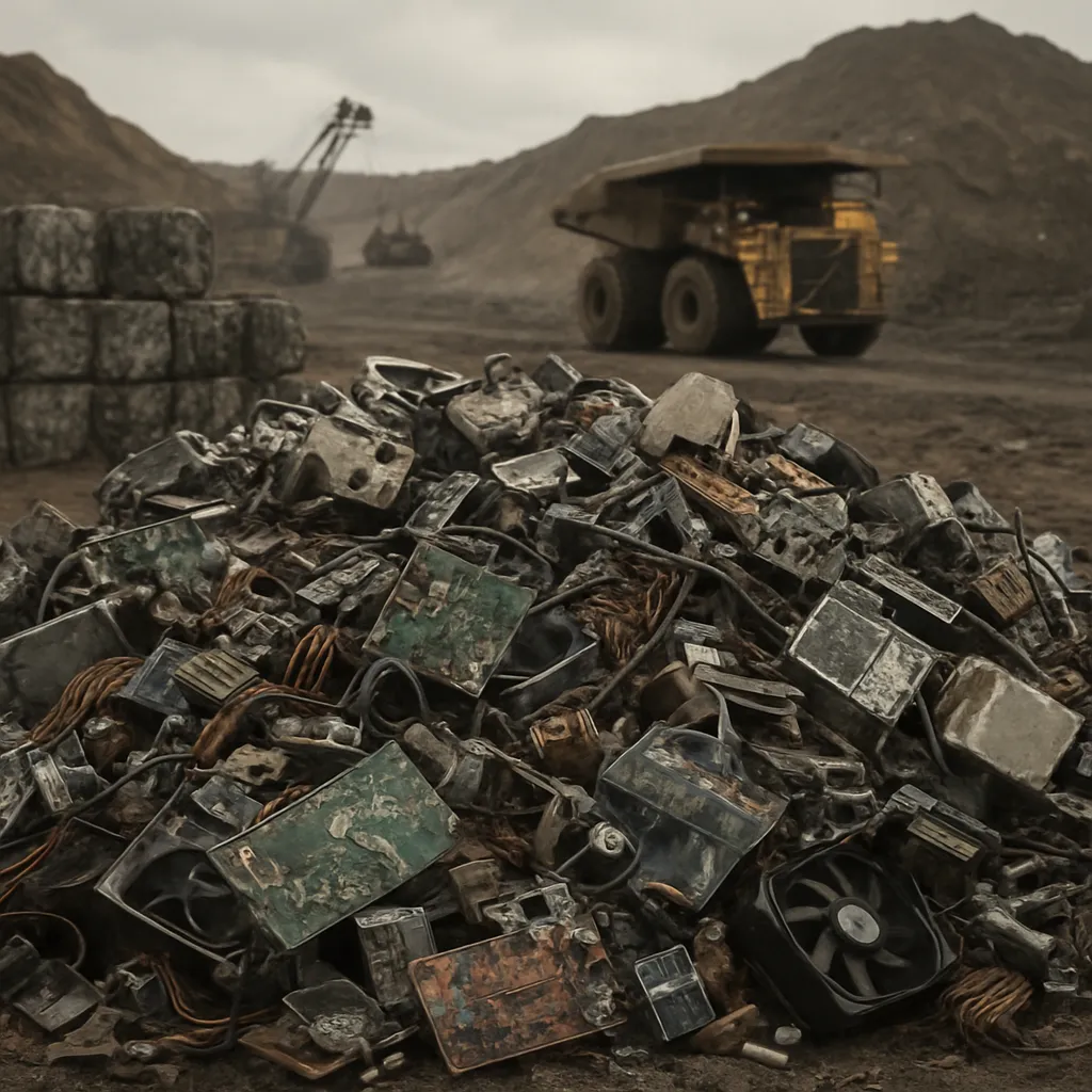
Closed-loop manufacturing is emerging as a vital pillar in the quest for sustainability. Techniques such as acid leaching, electrochemical extraction and plasma separation are being refined to recover gallium, indium and other rare elements from spent wafers and scrap materials. Early adopters report recovery rates exceeding 80 percent for certain materials, translating into significant cost savings and reduced environmental impact.
Industry consortia are standardizing protocols for collecting, sorting and processing electronic waste. Automated disassembly stations equipped with robotics and computer vision accelerate the separation of valuable substrates from bulk silicon and organic interlayers. Recovered metals are then sent to proprietary plants where advanced purification methods—such as zone refining and solvent extraction—recreate semiconductor-grade materials ready for reuse.
Benefits of a Circular Model
- Resource efficiency: Lower dependence on virgin mining reduces land disruption and carbon emissions.
- Supply security: Localized recycling facilities mitigate risks associated with long-distance shipping and geopolitical bottlenecks.
- Economic incentives: Recovered metals often command lower unit costs compared to freshly mined equivalents.
In tandem, governmental bodies are rolling out deposit-return schemes and recycling mandates to ensure high collection rates. Such regulatory frameworks, combined with corporate commitments, are setting the stage for a more resilient and recycling-driven semiconductor ecosystem.
Future Outlook and Emerging Challenges
Looking ahead, the interplay of technology advancement and resource availability will define the trajectory of the semiconductor industry. As device dimensions shrink and performance expectations escalate, the demand for specialized innovation-enabling materials will only intensify. At the same time, evolving climate policies and social expectations will exert mounting pressure on both miners and chipmakers to adopt greener, more transparent operations.
Efforts to deploy artificial intelligence in material discovery promise to accelerate the identification of novel alloys and substitutes. Meanwhile, cross-sector collaborations—from automotive to renewable energy—are spurring the development of shared recycling infrastructure capable of handling diverse waste streams. Through these concerted actions, the industry seeks to weave resilience into its very fabric, ensuring that the next generation of microelectronics can be built with stable, secure and environmentally responsible raw materials.